

Descriptions:
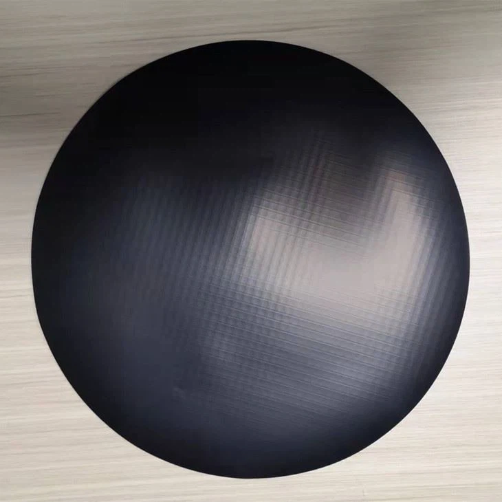
Conductive Wafer Pad of PS are constructed with high molecular superconduct graphene mixed high molecular polystyrene by propriety special process.
Uniform and stabled of surface resistances.
Excellence double-sides conduction performance.
Uniform bending resistance
All producing process in cleanroom environment
Packaging of vacuum and antistatic shield bags
Performance Characteristics:
Conductive Wafer Pad of PS
Type | Repousse 5x5mm square |
Surfaces resistances | 10x105~9Ω |

Applications:
Conductive Wafer Pad of PS are suitable to between wafer protective separator proformances
Conductive Wafer Pad of PS – (Interleaf) for use between individual wafers
Applicated for separat of wafer when shipping in container/ wafer jars
Work well as protective layer in between wafer during transportion
Suitable cleanroom environment : class 10~1000

Materials Information:
Conductive Wafer Pad of PS's material data
PS Conductive Wafer Separators | SSEM-20-BLK | 10E4-10E11 |
Order information: we are welcome customized
Conductive Wafer Pad of PS
Wafer size | Order code | Interleaf Diameter | Separators Thickness | Packaging |
4" | SSeIL0009-eM-20-BLK | 100mm | 0.13 mm (.005") | 200/pack |
5" | SSeIL0008-eM-20-BLK | 125mm | 0.13 mm (.005") | 200/pack |
6" | SSeIL0002-eM-20-BLK | 150mm | 0.13 mm (.005") | 200/pack |
8" | SSeIL0001-eM-20-BLK | 200mm | 0.13 mm (.005") | 200/pack |
12" | SSeIL0003-eM-20-BLK | 300mm | 0.13 mm (.005") | 200/pack |
FQA
Conductive Wafer Pad of PS
Q1. What is your term of payments?
T/T 30% as deposit at order time and balance 70% pay by before shipments.
Q2. How about your delivery time?
Generally, it takes 30~45 working days to get goods ready. The final lead time depends on the items and quantity of your order.
Q3.Can you produce according to the samples?
Yes, we can production according to your samples and technical drawings.
Q4.How do you make long-term business and relationships?
1. We keep good quality and competitive price to ensure our customers benefits.
2. We respect every customer as close partner and friends wherever they came from. We try best to satisfy our customers based on mutual benefit.
Hot Tags: conductive wafer pad, China, manufacturers, suppliers, factory, customized, wholesale, price, quality, quotation, in stock, free sample, made in China, cleanroom Printed Swabs, pc vacuum anti static, Cleanroom Printer Cleaning Swab, endust anti static wipes, cleanroompvafoam absorbentsponge, antistatic dust wipes
Materials Information:
Conductive Wafer Pad of PS
PS Conductive Wafer Separators | SSEM-20-BLK | 10E4-10E11 |


